Crazy H100: A brief analysis of modern GPU architecture
Thanks to the new wave of AI triggered by ChatGPT, major technology companies will purchase large quantities of H100 and other series of GPUs produced by NVIDIA in 2023. According to NVIDIA’s fiscal 2024 second quarter financial report1, NVIDIA’s revenue hit a record high, reaching US $ 13.507 billion, far exceeding analysts’ expectations of US $ 11.04 billion. The current market demand for H100 is around 432,000 units, each priced at about US $ 35,000. Limited by TSMC’s production capacity, NVIDIA H100 production in 2023 has already been sold out, and the current shortage of GPUs may continue until 2024 2.
On eBay, the price of an NVIDIA H100 SXM 80GB GPU is currently (2023.10) up to US $ 45,0003. At the same time, CoreWeave, which is valued at only US $ 2 billion, used NVIDIA H100 as collateral, but received US $2.3 billion in debt financing4. You know, CoreWeave currently does not have so many equivalent NVIDIA H100s, it only has NVIDIA’s H100 supply commitment. Just like the Chinese land finance boom in the past two decades, real estate developers can quickly mortgage the land obtained through land auctions and obtain bank loans. NVIDIA H100 has become as hard currency as land.

This article attempts to go deep into the hardware, starting with the NVIDIA H100 series GPUs, analyzing the modern GPU architecture, and trying to understand why the H100, which is so expensive, is still selling so well when large models continue to surge. Before the official start, we can listen to the song “GPUs Are Fire” 5 by GPU Utils to feel everyone’s enthusiasm for H100.
TLDR
- All the information in this article comes from public information on the Internet. It is more about understanding the architecture of modern GPU from a programmer’s perspective. It is strongly recommended that you read the original information in the appendix of this article. The opinions in this article have nothing to do with my employer.
- In addition to NVIDIA GPUs represented by H100, there are many other types of GPUs competing in the market: such as GPUs from AMD and Intel, Huawei’s Ascend 910 AI acceleration chip, Google’s TPU, AWS self-developed Tranium and Inferentia , and even GPUs from startups such as Biren. Because I mainly use NVIDIA GPUs in my work, this article also focuses on NVIDIA’s H100.
- With the development of the times, GPU, which was first originated from the field of graphics rendering, continues to travel in the three fields of HPC, graphics and deep learning. In the past few years, it also played an important role in cryptocurrency. This article will not introduce its graphics rendering capabilities in detail, but will focus more on the evolution and development of computing side capabilities. ** Due to space limitations, this article will not cover new features such as MIG and confidential computing, nor will it cover communication capabilities such as NVLink.
- As a software engineer, the author of this article does not have a deep and comprehensive understanding of hardware. There may even be deviations and errors. There will definitely be omissions when introducing relevant directions. Everyone is welcome to communicate and make corrections.
- This article is relatively long, with nearly 10,000 words in total, and it is expected to take about 20 minutes to read. It is recommended to follow, collect and watch it. You can also visit my blog for a better reading experience https://loop.houmin.site/context/gpu-arch-en.
Technical Terms
Before we really start, here is a brief introduction to the technical abbreviations that you may encounter in this article. You don’t need to deeply understand their meanings now, you just need to have a preliminary impression.
| English | Abbreviation | Chinese definition |
|---|---|---|
| FLOPS | Floating point Operations per Second | FLOPS is the number of floating point operations per second, and FLOPs represents the number of floating point operations |
| DGX | Deep-learning GPU Accelerator | A series of high-performance computing platforms launched by NVIDIA specifically designed to accelerate deep learning workloads |
| HGX | High-Performance GPU Accelerator | Server reference platform launched by NVIDIA. Used by OEMs to build 4 GPU or 8 GPU servers, manufactured by third-party OEMs such as Supermicro |
| SXM6 | Server PCI Express Module | NVIDIA’s high-bandwidth socket interface for connecting to GPU. Compared with PCIe, it has the characteristics of high bandwidth, low latency, high scalability, direct interconnection, etc. |
| HBM | High Bandwidth Memory | An advanced memory technology, compared with GDDR, etc., it has the characteristics of high bandwidth, low power consumption, and compact packaging |
| CoWoS7 | Chip on wafer on Substrate | Three-dimensional stacking, compared with GDDR, etc., has the characteristics of high bandwidth, low power consumption, and compact packaging |
| GPC | Graphics Processor Cluster | Graphics Processing Cluster, each GPC contains several TPCs |
| TPC | Texture Processor Cluster | Texture Processing Cluster, each TPC contains several SMs |
| SM | Streaming MultiProcessor | The core computing unit in the NVIDIA GPU architecture, responsible for executing parallel computing tasks |
| SIMT | Single Instruction Multiple Thread | Single instruction multi-threading, a parallel computing model in NVIDIA GPU, combines SIMD and multi-threading so that multiple threads can execute the same instruction at the same time but process different data |
| GEMM | General Matrix Multiplication | General matrix multiplication is a computational operation widely used in deep learning neural network models |
| MMA | Matrix Multiply-Accumulate | Matrix Multiply-Accumulate |
| FMA | Fused Multiply-Accumulate | Fused matrix multiplication and accumulation, realizing matrix multiplication and accumulation through a single instruction |
| TMA | Tensor Memory Accelerator | Tensor Memory Accelerator |
| MIG | Multi-Instance GPU | Multi-Instance GPU |
| TEE | Trusted Execution Environments | Trusted Execution Environments |
| DSA | Domain Specific Architecture | Domain-specific architecture is a chip architecture optimized for specific application scenarios, aiming to improve the performance and efficiency of the chip |
How many cards are needed for large model training?
**The expensive H100 cards are so expensive in Luoyang that demand exceeds supply. How many cards are needed for large model training? ** GPT-4 is most likely trained on 10,000 to 20,000 A100s 8. According to Elon Musk, GPT-5 training may require 30,000 to 50,000 H100s. Although it was later denied by Sam Altman, it can also be seen that large model training requires huge computing power.
Inflection announced that they are building the world’s largest AI cluster, containing 22,000 NVIDIA H100s. The FP16 computing power can reach 22 exaFLOPS. If lower-precision computing power (that is, FP8) is used, higher computing power can be obtained [ ^6]. This is a very astonishing number, considering that the Frontier supercomputer is currently the only supercomputer that has reached the ExaFLOPS level of computing power. Compared with the Sunway TaihuLight supercomputer, currently ranked seventh, the maximum computing power is only 94.64 PetaFlOPS. Inflection proudly claims that if they participate in the Top 500 supercomputer rankings9, they can easily rank second and approach the number one Frontier supercomputer.
The deployment of 22,000 NVIDIA H100 GPUs in one cluster is truly unprecedented, and will support training and deployment of a new generation of large-scale AI models. Combined, the cluster develops a staggering 22 exaFLOPS in the 16-bit precision mode, and even more if lower precision is utilized. 10
Based on more than 3,500 NVIDIA H100 images, Inflection took less than 11 minutes to train the GPT-3 model under the C4 data set 11. Compared with OpenAI, which used thousands of NVIDIA V100s to train GPT-3 in 2020, it took about a month. Compared with V100, the computing power of H100 has increased significantly. The screenshots here are not complete, but only roughly reflect the manufacturers and systems currently participating in Benchmark12.

For an AI cluster composed of 22,000 NVIDIA H100s, the US$1.3 billion invested by Microsoft and NVIDIA in Inflection may have cost more than half. This scene is surprising. There may be a bubble, but real money will not lie. Let us also think carefully about why we need so many cards. OpenAI proposed an empirical formula for us in the Scaling Laws13 paper as early as 2020:
$$ C = \tau T \approx 6 * P * D $$
Here:
- $C$ is the computing power required to train a Transformer model, the unit is FLOPs
- $P$ is the number of parameters in a Transformer model
- $D$ is the size of the training data set, that is, how many tokens are used for training
- $\tau$ refers to the total computing throughput of all hardware in the training cluster, the unit is FLOPs, and the calculation method is $\tau = (No. GPUs) * (Actual FLOPs/GPU)$
- $T$ refers to the time required to train this model, the unit is seconds
Scaling Law Paper Section 2.1 made a simple derivation of this formula. The number of FLOPs required in the forward pass is $C_{forward} = 2 * P * N$. The number of FLOPs required in the backward pass is roughly twice that of the forward pass. , so $C_{backward} = 4 * P * N$, which is the source of the coefficient 6.
The reason for such a concise formula is that whether it is bias vector addition, layer normalization, residual connections, non-linearities, softmax, or even attention calculation, it is not the main factor accounting for computing power. The most critical factor is Transformer. Matrix operations in **.

After remembering the above assumptions, we can simply calculate the coefficient 6 here, 2 times in the forward direction and 4 times in the reverse direction, as shown in the figure below.
![]()
This empirical formula has been verified again in the GPT-3 paper. It can be seen that for the transformer model with a decoder-only structure such as GPT-3, the FLOPs required for each parameter and each token are 6. For the transformer model with encoder-decoder structure such as T5, in the forward pass and backward pass, because only half of the parameters for each token are active, the coefficient in this empirical formula is 3.

When calculating the required computing power, we just used the unit of FLOPS, which is FLOP-seconds. In the Scaling Laws paper, we tend to use the unit of PetaFLOP-days, so that we can more intuitively feel how long it takes to train a model. time. Take LLaMA-1, which was open sourced by Meta at the beginning of the year, as an example. The 65B model is trained based on 1.4T tokens and uses 2048 NVIDIA A100 GPUs. So how long does it take to train?
- Required computing power $C = 6 * N * P = 6 * 65 e^9 * 1.4 e^{12} = 546e^{21} FLOPs$
- NVIDIA A100 WhitePaper gives the computing power of BF16 Tensor Core as 312 TFLOPS15, but in fact the computing power is generally between 130 and 180 TFLOPS. Here we take the middle value of 150 TFLOPS16
- The cluster computing throughput calculated based on the actual computing power is $\tau = 2048 * 150e^{12} = 300e^{15} FLOPS$
- The time required to train LLaMA-1 is $T = \frac{C}{\tau} = \frac{546e^{21}}{300e^{15}} = 1.82e^6 Seconds \approx 21 days$
This calculation is basically consistent with the actual training time of LLaMA-1 in the paper:
When training a 65B-parameter model, our code processes around 380 tokens/sec/GPU on 2048 A100 GPU with 80GB of RAM. This means that training over our dataset containing 1.4T tokens takes approximately 21 days.

Further calculations show that NVIDIA H100 WhitePaper gives BF16 1979 TFLOPS. Because this indicator includes sparsity, the actual dense computing power is approximately 1000 TFLOPS17. Compared with A100, there is almost a 3-fold increase. So with the same number of GPUs, without considering other factors and doing the roughest calculations, the training time of LLaMA-1 65B can be reduced to less than 10 days 18. Considering the computing power of H100’s newly launched FP8 Tensor Core 3,958 TFLOPS and the communication bandwidth of the new generation NVLink Network, the training speed can be further accelerated. GPT-3 175B training can be more than 6 times faster than the A100.

In addition to its obvious advantages over the A100 in terms of performance, the H100 is also superior to the A100 in terms of cost. Although the unit cost of H100 is 1.5 to 2 times that of A100, the efficiency is 3 times that of A100, so the performance per dollar of H100 is higher than that of A100. This is what Lao Huang said “The More You Buy, The More You Save”, NVIDIA is winning🐶

Through the above calculation, we can see the huge demand for GPUs in LLM training, and also see the huge advantages of H100 over A100. This is one of the reasons why H100 is currently in short supply. Next, this article will try to delve into the H100 hardware and see how H100 is better than A100.
The H100 series product line
NVIDIA’s product line is relatively complex, ranging from data centers to professional workstations, as well as consumer-grade GPUs and embedded scenarios. The names of its series of products are also relatively complex, which you can see here19.
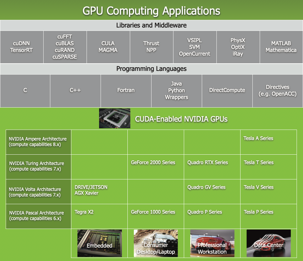
This article mainly focuses on the data center H100 series product line. Before going into the specific hardware architecture, let’s first take a look at the appearance of NVIDIA’s H100-based series product line and get a rough impression of HGX and DGX.


It is worth noting that these four NVSwitch Gen3 chips have a total of 3.6 TFLOPS of SHARP In-Network Computing computing power, which is not listed here for the time being. I will write an article to talk about SHARP later.

Of course, DGX H100 SuperPod can also go further with ScaleUp, which is called NVIDIA EOS. I won’t go into it further here (no money😭). The previous pictures can basically show the NVIDIA H100 series product line. You can further understand it more clearly through the following video Learn about its composition, or check out Lao Huang’s report at the 2022 GTC spring conference20.


CUDA programming model and H100 architecture
This section will combine the NVIDIA CUDA programming model with a comparative analysis of the H100 GPU architecture. As shown in the figure below, the fully configured GH100 has 8 GPCs, each GPC has 9 TPCs, and each TPC has 2 SMs, for a total of 144 SMs. The SXM5-based H100 has cut off 6 TPCs and has only 66 TPCs, for a total of 132 SMs.

H100 supports the fourth generation NVLink and PCIe Gen5, supports 6 HBM3 Stacks, DRAM bandwidth reaches 3TB/s, and L2 Cache reaches 50MB.

Continue to zoom in on each SM to see its composition:
| Functions in SM | Component Name | Unit per SM |
|---|---|---|
| Computing | CUDA Core FP32 Unit | 128, divided into four groups, 32 in each group |
| Computing | CUDA Core FP64 Unit | 64, divided into four groups, 16 in each group |
| Computing | CUDA Core INT32 Unit | 64, divided into four groups, 16 in each group |
| Computing | TensorCore Gen4 | 4, divided into four groups, 1 in each group |
| Computing | SFU | 4, divided into four groups, 1 in each group |
| Computing | Tex | 4, divided into four groups, 1 in each group |
| Scheduling | WARP Scheduler | 4, divided into four groups, 1 in each group, 32 thread/clk |
| Scheduling | Dispatch Unit | 4, divided into four groups, 1 in each group, 32 thread/clk |
| Storage | Register File | 256KB, divided into four groups of 64 KB each |
| Storage | L0 Instruction Cache | – |
| Storage | L1 Data Cache/Shared Memory | 256KB |
| Storage | L1 Instruction Cache | – |
| Storage | LD/ST | 32, divided into four groups, 8 in each group |
| Storage+Computing | Tensor Memory Accelerator | 1 |
- Contains 128 CUDA Cores, divided into 4 groups, each group contains 16 FP64 Units, 16 INT32 Units and 32 FP32 Units. These CUDA Core units can be used for calculations in supercomputing, graphics rendering and other scenarios.
- Contains the fourth generation Tensor Core, which is temporarily skipped here and will be introduced in detail in the Tensor Core section.

GH100 Streaming Multiprocessor(SM), Source: NVIDIA H100 WhitePaper
People with trypophobia may be a little scared when they see the dense computing core of SM. In order to better understand the structure of NVIDIA GPU, we can look at the simplified version below:
- For each GPU, it can be divided into many SMs through the levels of GPC and TPC
- SM can be further divided into 4 groups, each group has its own 64KB Register File and many computing cores.
- All threads running in the same SM share 256KB Shared Memory and L1 Data Cache
- All SMs in the same GPU share 50MB L2 Cache and 80GB HBM3 Memory
- Looking further outward, GPUs on the same node are connected together through NVLink/NVSwitch

In this picture, we have seen that corresponding to the hardware, from the perspective of the CUDA programming model at the software level, we further introduce the CUDA programming model. In the CUDA programming model, the CPU and main memory are called Host, and the GPU and video memory are called Device. The CUDA program contains both Host program and Device program, which run on the CPU and GPU respectively.
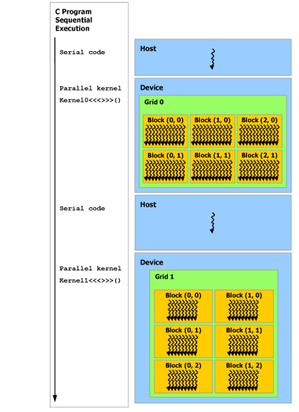
In order to implement GPU parallel accelerated computing, we need to execute kernel launch on the Host so that the kernel function can be executed concurrently on multiple threads on the Device. CUDA calls the operation defined by the kernel function Thread, multiple threads form a Block, and multiple blocks form a Grid. The specific method is to specify the number N of threads to be executed by the kernel function through <<<grid, block>>> when calling the kernel function. After that, the N Cores on the GPU will execute the kernel function in parallel, and each thread A unique thread number threadID will be assigned. This ID value can be obtained through the built-in variable threadIdx of the kernel function.
A thread needs two built-in coordinate variables (blockIdx, threadIdx) to uniquely identify them. They are both dim3 type variables, where blockIdx indicates the location of the thread in the grid, and threadIdx indicates the location of the thread in the block. The following is a typical matrix multiplication CUDA program example. The block size is defined as 16 x 16, that is, each block has 256 threads. The value of grid is calculated based on the size of the matrix to calculate how many blocks are needed.
|
|
In order to further understand the CUDA programming model concept and hardware structure here, we continue to talk about the WARP Scheduler that was not mentioned just now. NVIDIA SM adopts SIMT architecture 21. The thread bundle warp is the most basic execution and scheduling unit. A warp generally contains 32 threads. These threads execute the same instructions with different data resources.
| CUDA Perspective | Features | Hardware Perspective |
|---|---|---|
| Thread | The smallest computing unit, each thread has its own program counter and status register | Corresponding to Core, or lanes |
| warp | The smallest execution and scheduling unit, an SM’s CUDA Core will be divided into several warps | Warp Scheduler schedules one warp at a time |
| block | Warps in a block can only be scheduled in the same SM | Corresponding to SM, threads in a warp must be scheduled in the same block |
| grid | a GPU | corresponds to the GPU |
Although threads in a warp execute the same program address, they may have different behaviors, such as branch structures. Because the GPU stipulates that all threads in a warp execute the same instructions in the same cycle, warp divergence will cause performance degradation. The concurrent warps of an SM are limited. Due to resource limitations, SM must allocate shared memory for each thread block, and also allocate independent registers for the threads in each thread warp, so the SM configuration will Affects the number of thread blocks and warp concurrency it supports.

Warps of the same block can only be scheduled to run on the same SM, but the same SM can accommodate multiple warps from different blocks. In the mainstream architecture, each SM has a maximum of 2048 threads, which is a maximum of 64 warps. An SM consists of 4 groups of warp schedulers, and whichever warp is ready will be scheduled. Generally, a warp may not be ready because it is waiting for memory transfer, computing core, or sync. After the warp is scheduled, you can go to the dispatch unit.

So far, the CUDA programming model introduced earlier is actually an abstraction before the Hopper architecture, that is, grid/block two-level scheduling, and block is mapped to SM. With the introduction of Cooperative Groups and the support of asynchronous programming, multiple Kernels communicate with each other in the form of producers and consumers, and the communication bandwidth from SM to SM is also increasing.

In the Hopper architecture, the concept of Distributed Shared Memory (DSMEM) is added. The SM within a GPC has dedicated communication bandwidth, so a new layer of Cluster scheduling layer is added to CUDA.


With the cluster abstraction, threads similar to the same block will be scheduled to the same SM, and thread blocks of the same cluster will be scheduled to the same GPC.

In this way, threads in different blocks in the same cluster can access the DSMEM of another block through the SM to SM Network. In this way, it becomes very simple to implement LD/ST, Atomic, Reduce and asynchronous DMA operations of multiple SMs within a GPC.

The memory model from the CUDA programming model becomes as shown in the figure below:
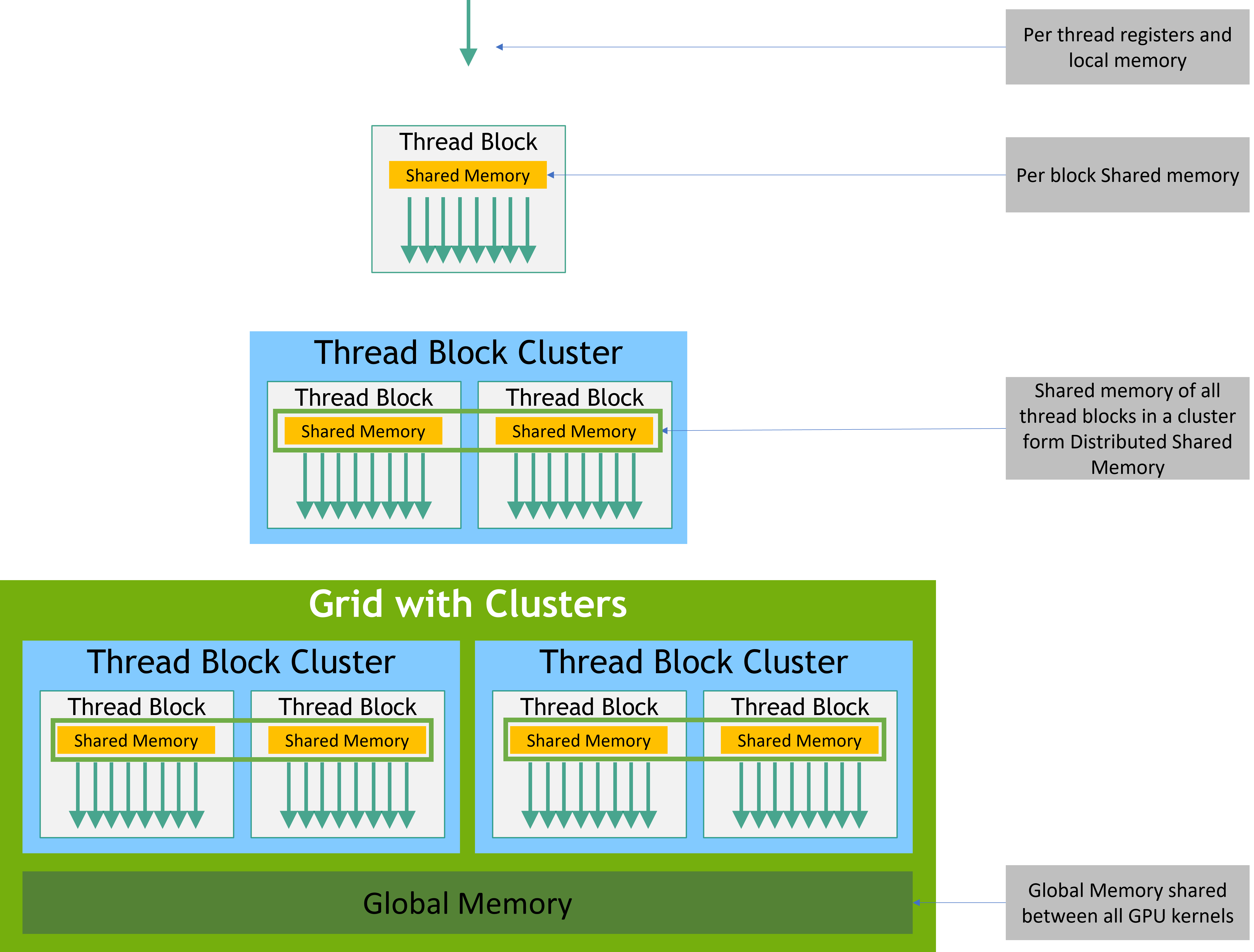
In essence, CUDA introduces the abstraction of block and cluster to better utilize the principle of spatial locality. Block allows all threads to be scheduled to the same SM, allowing threads to quickly synchronize through fast barriers and exchange data through the Shared Memory of the SM. As GPUs have more and more SMs, only using the Block layer of abstraction can no longer make better use of the locality principle. Therefore, Hopper introduced the Cluster layer of abstraction to allow all threads to run within the same GPC.
Summary: This section briefly introduces the NVIDIA CUDA programming model and the corresponding GPU hardware architecture. In fact, NVIDIA’s hardware architecture is constantly changing, from the SIMT model of the earliest Telsa architecture to the introduction of an independent program counter PC for each Thread in the Volta architecture, to the later introduction of Cooperative Groups and asynchronous programming APIs. These designs It was made after various tradeoffs and tradeoffs. Regarding the evolution of NVIDIA series GPU architecture, I highly recommend zartbot’s series of articles 22.
The evolution of CUDA Core and Tensor Core
In deep learning, there are a lot of calculations of $Y = X * W + B$, which are then passed to the next layer of neural network through the activation function. This is a typical GEMM operation. The optimization of GEMM is a very interesting topic, from the mathematical perspective of optimization of algorithms such as Strassen, to the computer perspective of optimization using principles such as memory access locality 23, and even various hardware levels. The optimization can be done very deeply.
In 2016, Google released TPU24, which optimizes matrix multiplication in hardware based on the ancient technology of systolic array25, which set off the clarion call for various DSA AI chips to challenge NVIDIA GPUs. NVIDIA, which has been moving forward on the SIMT road, actively responded to the challenge. At the climax of the last wave of deep learning hustle and bustle, which was the release of the Volta architecture in 2017, it began to embark on the path of DSA and introduced Tensor Core.

Unlike CUDA Core, which can only perform one floating-point multiplication calculation per unit clock cycle, Tensor Core can perform one matrix multiplication calculation per unit time. Taking the Volta architecture as an example, Tensor Core can support 4 x 4 x 4 mixed-precision multiplication and accumulation per clock cycle, where the A matrix and B matrix are both FP16 precision, and the C matrix and D matrix are FP16 or FP32 precision.


The Turing architecture adds support for INT8/INT4/INT1 data types.

New BF16 and TF32 data types were added to the Ampere architecture, and support for Sparsity was added, and the mixed-precision matrix multiplication and addition supported by each TensorCore in each clock cycle evolved from Volta’s 4 x 4 x 4 to 8 x 4 x 8 .

The BF16 data format is a truncated (16-bit) version of the 32-bit IEEE 754 single-precision floating-point format (float32). It preserves the approximate dynamic range of a 32-bit floating point number, retains 8 bits of the exponent, but supports only a 7-bit mantissa. Bfloat16 is used to reduce storage requirements and improve the calculation speed of machine learning algorithms 26.

The new TF32 will not encounter the overflow problem like FP16. At the same time, with the new BF16 and FP32, the step accuracy can be improved, and for a multiplier, the chip area is saved.

As a result, the computing power is further increased:

With the Hopper architecture, the mixed-precision matrix multiplication and addition supported by each TensorCore per clock cycle has evolved to 4 x 8 x 16. TF32, FP64, and INT8 Tensor Core have a 3x performance improvement compared to Ampere.


The most important thing is that NVIDIA introduced the FP8 data type in the Hopper architecture TensorCore and proposed the Transformer Engine technology for the Transformer architecture. We will further elaborate on this in the next section and will not list it here.


FP8 mixed precision training and Transformer Engine
As mentioned before, an important feature of the Hopper architecture is that TensorCore introduces the FP8 data type, which is also a huge advantage of H100 over A100.
- Accelerate math-intensive operations: Due to low precision, FP8 is 2 times faster than 16-bits TensorCore.
- Accelerate memory-intensive operations: Because it only occupies one byte, FP8 can significantly reduce access to storage traffic compared to 16-bits, and can also reduce the memory footprint of the model.
- More convenient for inference: Using FP8 in inference is already a very popular choice. When training in FP8 format, it can be more convenient for inference deployment, and there is no need to further quantify the model.

FP8 in Tensor Core supports two data formats:
-E4M3
- Does not follow the IEEE 754 standard, supports NaN and Zero encoding, but does not support Inf
- Data accuracy is relatively higher and can be used for fwd pass and inference
- E5M2:
- Comply with IEEE 754 standard and support encoding of Inf, NaN and Zero
- Wider range of data, gradient representation available for mixed precision training

The following figure shows the main process diagram of FP8 GEMM calculation:

In this paper 28, NVIDIA, ARM and Intel used FP8 mixed precision training to conduct verification under different network structures such as Transformer-based language model and CNN-based visual model, proving that FP8 can be basically consistent with BF16 Effect.
![]()
Having said so much about FP8 mixed precision training, what is the Transformer Engine in the H100 white paper? In fact, Transformer Engine does not involve a dedicated hardware structure, but a library that accelerates Transformer training at the software level 29, which provides an acceleration solution for FP8 mixed precision training. Transformer Engine can essentially dynamically adjust floating point precision through the value range of label output. This will not be discussed in detail here. You can refer to the official documentation of Transformer Engine 30.
![]()
The Nvidia Empire State Building is complete, with only a few dark clouds overhead.
30 years ago, NVIDIA was founded. 30 years later, NVIDIA’s market value exceeded one trillion US dollars and it built its own huge empire. Standing today in 2023, looking back at the development of the GPU market in the past thirty years, it is full of emotions:
- 1983 The Great Depression of American video games31 and the introduction of personal computers in the 1980s allowed games to move from the original home game consoles to the PC platform, thus triggering the demand for graphics cards under the PC platform. NVIDIA was struggling in the early days of its establishment in 1993. It was with funding from the Japanese arcade game company Sega and betting on Microsoft’s DirectX interface that the RIVA launched quickly gained market recognition and further launched the world’s first GPU GeForce 256, completely Stand firm in the market. In that era of chaos from 1990 to 2000:
- Graphics card pioneer 3DFX was eventually acquired by NVIDIA
- S3 was acquired by VIA and gradually became silent
- Intel finally gave up on independent graphics to focus on integrated graphics. This plot recurred again in the 2000s. It wasn’t until 2018 that Intel truly realized what they had lost and started producing independent graphics cards again.
- ATI continued to fight with NVIDIA and was eventually acquired by AMD. After some integration, AMD is still on the front line of competition today.
- From the 2000s to the 2010s, NVIDIA and ATI competed for the supremacy of programmable GPUs. NVIDIA launched the extremely flexible and programmable CUDA architecture in 2006 and has firmly continued on this path, building its largest moat today.
- In the 2010s, with the arrival of the mobile Internet wave, NVIDIA launched the TEGRA mobile processor in an attempt to get involved in this market, but ended in failure. Fortunately, deep learning began to rise after 2012, and NVIDIA quickly seized this wave of opportunities. CUDA eventually dominated this market, and AMD’s ROCm is still struggling to maintain it today. NVIDIA has continued to make rapid progress in this decade, seizing every market opportunity including cryptocurrency and autonomous driving, and achieving dominance in markets such as data centers, HPC, and professional graphics.
- After 2020, NVIDIA acquired Mellanox, combining powerful computing power with high-speed communication networks. NVIDIA told the story of DPU again, and continued to slowly cultivate its DOCA platform, trying to repeat the story of CUDA. It is a pity that NVIDIA’s acquisition of ARM was not approved in the end, and ARM was listed independently. Otherwise, NVIDIA, with its CPU, GPU and DPU, could really completely define the next generation of computing platforms.

Huang’s sword skills make everyone love and hate him. The former dragon slayer has become the new dragon. The H100 is now so expensive but sells so well. Teacher Xia Jing from Huawei Kunpeng analyzed the cost of the H100 32. The actual physical cost of the H100, which sells for more than 30,000 US dollars, may be less than 3,000 US dollars. This is also consistent with overseas investment. It is basically consistent with the US$3,320 analyzed by research institution Raymond James33. Looking at pure physical costs, the profit margin of H100 is close to 1000%. Although it is not fair to look at profit margins aside from R&D costs, it also shows NVIDIA’s confidence. This is really the best thing about Infra. I can sell it at a high price and I can define my own platform, but you still have to rush to use mine. The evil dragon is still there, the world has been suffering for a long time, and there are still new young people who want to defeat the evil dragon.
In June this year, AMD released the Instinct MI300 series, of which MI300X directly benchmarked NVIDIA H100. In an interview, Su Ma’s answer to the insurmountable moat problem of CUDA 34 reflects the industry’s strong dependence on the LLM field. The problem with NVIDIA is urgent.
Q: If you look at what Wall Street thinks Nvidia’s mode is, it’s CUDA… You have ROCm, which is a little different. Do you think that that’s a moat that you can overcome with better products or with a more open approach?
Lisa Su: I’m not a believer in moats when the market is moving as fast as it is… When you look at going forward, actually what you find is everyone’s looking for the ability to build hardware-agnostic software because people want choice. Frankly, people want choice… Things like PyTorch, for example, which tends to be that hardware-agnostic capability.
Q:PyTorch is a big deal, right? This is the language that all these models are actually coded in. I talk to a bunch of cloud CEOs. They don’t love their dependency on Nvidia as much as anybody doesn’t love being dependent on any one vendor. Is this a place where you can go work with those cloud providers and say, “We’re going to optimize our chips for PyTorch and not CUDA,” and developers can just run on PyTorch and pick whichever is best optimized?
Lisa Su: That’s exactly it. PyTorch really is trying to be that sort of hardware-agnostic layer — one of the major milestones that we’ve come up with is on PyTorch 2.0. But our goal is “may the best chip win.” And the way you do that is to make the software much more seamless. And it’s PyTorch, but it’s also Jax. It’s also some of the tools that OpenAI is bringing in with Triton.
CUDA is indeed very good, but is it so good that you have to pay too much cost for it, including actual monetary costs and various hidden costs. Based on the new generation of middle layers such as PyTorch or Jax, new solutions are being formed. “AMD AI Software Solved – MI300X Pricing, Performance, PyTorch 2.0, FlashAttention, OpenAI Triton” This article 35 shows that based on PyTorch 2.0 and OpenAI Triton, MosaicML can implement basically no code modifications on the AMD hardware platform. NVIDIA A100 Basically consistent performance.

We profiled training throughput of MPT models from 1B to 13B parameters and found that the per-GPU-throughput of MI250 was within 80% of the A100-40GB and within 73% of the A100-80GB.
Abhi Venigalla, MosaicML36
In July this year, Intel released the Habana Gaudi 2 AI chip in China, hoping to get a share of this wave of generative artificial intelligence when the sale of NVIDIA H100/A100 is banned in China. Habana Gaudi 2 is Intel’s work after acquiring Habana Labs in 2019. It is also Intel’s second attempt after wasting 3 years on acquiring Nervana.
In addition to NVIDIA, AMD, and Intel, the three old enemies who are working together in various fields such as CPU/GPU/DPU, there are also AI Chip startups such as GraphCore and Cerebras that are still going on.

At the same time, cloud service giants have huge businesses and are naturally not willing to be controlled by others, so they have invested in self-developed AI chips. Not long ago, AWS invested US$4 billion in Anthropic37. One of the goals is to make AWS’s self-developed Trainium and Inferentia widely used38. At the end of August, Google Cloud’s H100 instance A3 finally arrived, but maybe this is not their focus. The focus is that they released TPUv5e39. As a pioneer in AI chips, Google’s TPU is much more mature than AWS’s Trainium/Inferentia, and TPU is also a strong competitor against NVIDIA H100 40.
The NVIDIA Empire State Building has been built, but there are still a few dark clouds overhead. Now that the United States has banned the sale of A100/H100, domestic AI chips such as Huawei’s Ascend 910 are slowly beginning to be used. Thirty years ago, facing the paradigm shift of the new computing platform of personal computers, giants like Intel, Microsoft and NVIDIA were born. Today, 30 years later, a new wave of generative artificial intelligence may usher in a new computing paradigm shift. What will the story be like when facing the dragon this time?
-
https://nvidianews.nvidia.com/news/nvidia-announces-financial-results-for-second-quarter-fiscal-2024 ↩︎
-
https://gpus.llm-utils.org/nvidia-h100-gpus-supply-and-demand/ ↩︎
-
Tesla H100 80GB NVIDIA Deep Learning GPU Compute Graphics Card, 2023-08-30, ebay, https://www.ebay.com/itm/334736271213 ↩︎
-
https://www.coreweave.com/blog/coreweave-secures-2-3-billion-debt-financing-magnetar-capital-blackstone ↩︎
-
SXM socket, https://en.wikipedia.org/wiki/SXM_ (socket) ↩︎
-
CoWoS, TSMC, https://3dfabric.tsmc.com/english/dedicatedFoundry/technology/cowos.htm ↩︎
-
https://www.fierceelectronics.com/sensors/chatgpt-runs-10k-nvidia-training-gpus-potential-thousands-more ↩︎
-
Inflection AI builds the largest AI cluster in the world, Inflection, https://inflection.ai/inflection-ai-announces-1-3-billion-of-funding ↩︎
-
Announcing our collaboration with NVIDIA and CoreWeave on MLPerf, Inflection, https://inflection.ai/nvidia-coreweave-mlperf ↩︎
-
Scaling Laws for Neural Language Models, Jared Kaplan etc, https://arxiv.org/abs/2001.08361 ↩︎
-
The FLOPs Calculus of Language Model Training, Dzmitry Bahdanau, https://medium.com/@dzmitrybahdanau/the-flops-calculus-of-language-model-training-3b19c1f025e4 ↩︎
-
NVIDIA Ampere WhitePaper, https://www.nvidia.com/en-us/data-center/a100 ↩︎
-
Transformer Math 101, EleutherAI, https://blog.eleuther.ai/transformer-math/ ↩︎
-
Benchmarking Large Language Models on NVIDIA H100 GPUs with CoreWeave (Part 1), MosaicML, https://www.mosaicml.com/blog/coreweave-nvidia-h100-part-1 ↩︎
-
Andromeda Cluster: 10 exaflops* for startups, https://twitter.com/natfriedman/status/1668650915505803266 ↩︎
-
https://en.wikipedia.org/wiki/List_of_Nvidia_graphics_processing_units ↩︎
-
GTC 2022 Spring Keynote with NVIDIA CEO Jensen Huang, https://youtu.be/39ubNuxnrK8?t=1633 ↩︎
-
NVIDIA CUDA SIMT Architecture, https://docs.nvidia.com/cuda/cuda-c-programming-guide/index.html#simt-architecture ↩︎
-
History of GPU architecture evolution, zartbot, https://mp.weixin.qq.com/s/ThLUh-tv0h9mjfz9-0TlxA ↩︎
-
https://cloud.google.com/blog/products/ai-machine-learning/an-in-depth-look-at-googles-first-tensor-processing-unit-tpu ↩︎
-
Pulsating Array - Reborn with Google TPU, Tang Shan, https://zhuanlan.zhihu.com/p/26522315 ↩︎
-
A Study of BFLOAT16 for Deep Learning Training, https://arxiv.org/abs/1905.12322 ↩︎
-
https://developer.nvidia.com/blog/programming-tensor-cores-cuda-9/ ↩︎
-
FP8 Formats for Deep Learning, NVIDA, Intel and Arm, https://arxiv.org/abs/2209.05433 ↩︎
-
https://docs.nvidia.com/deeplearning/transformer-engine/user-guide/examples/fp8_primer.html ↩︎
-
Talk about the failure of the NVIDIA empire, Xia Jing, https://zhuanlan.zhihu.com/p/63918157 ↩︎
-
https://www.tipranks.com/news/article/nvidia-and-amd-are-both-strong-buys-says-raymond-james ↩︎
-
https://www.theverge.com/23894647/amd-ceo-lisa-su-ai-chips-nvidia-supply-chain-interview-decoder ↩︎
-
AMD AI Software Solved – MI300X Pricing, Performance, PyTorch 2.0, FlashAttention, OpenAI Triton, https://www.semianalysis.com/p/amd-ai-software-solved-mi300x-pricing ↩︎
-
Training LLMs with AMD MI250 GPUs and MosaicML, https://www.mosaicml.com/blog/amd-mi250 ↩︎
-
Expanding access to safer AI with Amazon, https://www.anthropic.com/index/anthropic-amazon ↩︎
-
Amazon Anthropic: Poison Pill or Empire Strikes Back, https://www.semianalysis.com/p/amazon-anthropic-poison-pill-or-empire ↩︎
-
Expanding our AI-optimized infrastructure portfolio: Introducing Cloud TPUv5e and announcing A3 GA, https://cloud.google.com/blog/products/compute/announcing-cloud-tpu-v5e-and-a3-gpus-in-ga ↩︎
-
TPUv5e: The New Benchmark in Cost-Efficient Inference and Training for <200B Parameter Models, https://www.semianalysis.com/p/tpuv5e-the-new-benchmark-in-cost ↩︎

alipay

Author houminwei
Publish October 10, 2023
LastMod February 15, 2024
License 本作品采用 CC BY-NC-ND 4.0 许可协议进行许可,转载时请注明原文链接
如果你在浏览博客的过程中发现了任何问题,欢迎在对应文章下评论。如果你有其他事情想要咨询,可以通过邮件联系我。